Ansys EMC Plus and Ansys Charge Plus 2025 R1 What’s New
2025 R1 updates are now available for Ansys EMC Plus and Ansys Charge Plus. This latest release includes performance updates and focuses on feedback from application engineers and software users.
Ansys EMC Plus
EMC Plus is a platform-level electromagnetic modeling and simulation tool that delivers a design to validation workflow. Application areas include electromagnetic environmental effects (E3), cables, EMI/EMC, and RF de-sense.
Key 25R1 updates are:
- Integration with Discovery materials
- Sub-cell multi-thin-layer materials
- Improved UX for large models
- Enhanced 3D visualization performance
- Clip plane for voxel mesh inspection
- Conformal boundary approximation (Beta)
- Automatic cable twisting
Conformal Boundary Approximation
Conformal boundary approximation (CBA) allows users to approximate curved surfaces better than using a cubic mesh. Cubic mesh creates a staircasing effect, Figure 1 on the left, which limits accuracy for surfaces that are not aligned with the main coordinate axis’ (X, Y, and Z). This leads to enhanced fields and inaccurate results. In Figure 1 on the right, we are creating a spark between two spheres and there is some field fluctuation and enhancement between the two due to staircasing, which changes the results of an ESD or air breakdown problem.

Fig. 1. Staircasing effect shown in a cubic mesh (left) and field function and enhancement caused due to staircasing (right).
Users can select CBA surfaces as an option to correct for the inaccuracies of the stair-case effect. CBA reduces errors while retaining the benefits of the Cartesian Yee Grid meshing scheme, making CBA essential to solving radome problems.
This is a beta feature and currently available for serial-CPU only. To use the feature, you need to go to tool settings and select ‘enable beta features,’ Figure 2. Upcoming in 25R2 the feature will be in parallelization and in GPU.

Fig. 2. How to turn on beta features in Ansys EMC Plus.
Thin Layer Materials Stackups
We have also introduced a thin layer capability in conjunction with CBA. This feature is key to solving radome applications and antenna systems with higher capabilities than what we have had in the past.
Users may now assign surfaces to contain multiple thin layers in an effective surface. Users can also easily change thickness, permittivity, and conductivity to capture how the fields are being affected both for reflection and transmission. The new solver algorithm is accurate without using as many computational cells.
It is available now in the materials tab, seen in the Figure 3.

Fig. 3. How to open the new thin layer materials feature.
Automatic Cable Twisting
Twisted pairs, twisted shielded pairs, twisted triples, and related constructions have important applications that require electromagnetic analysis. How they twist will impact any coupling of the electromagnetics to the system and change the currents and voltage. If you have various modes that you’re exploring in terms of coupling, twisting is going to be key.
EMC Plus now allows users to automatically twist cables in the solver. This makes manually segmenting cables a thing of the past. To get started, users will define the number of twists, and that information is automatically passed to the solver.
The capacitance and inductance matrix calculations for transmission line theory are calculated individually for each mesh segment of the cable instead of at the beginning and end of the full wire. This is going to be a steppingstone for different capabilities that we are working on for the future.
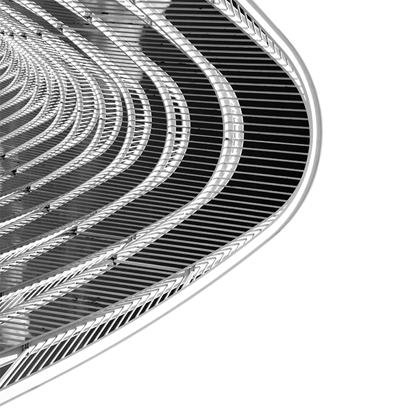
Clip Plane for Voxel Mesh Inspection
The clip plane is a brand-new mesh visualization capability. Clipping planes allow for interior mesh elements to be inspected. To do this, we changed how we render the mesh. Users can choose the axis on which to move the plane and see live changes in the visible voxels. Figure 4 shows two different views.

Fig. 4. Different views of the clipped plane mesh.
You can access this tool by clicking on the “clip plane” button in the EMA3D ribbon, shown in Figure 5. It is the purple box to the left of the mesh button.

Fig. 5. Find the clip plane button next to the mesh button in the EMA3D ribbon.
Figure 6 is an example of an F-16. One side is clipped is other is not. On the clipped side you can see cables and where they are being propagated through the system. This allows you to analyze any connectivity issues that you may have in your mesh and give you additional information about how to diagnose problems.
Ansys Charge Plus
Charge Plus combines electromagnetic solvers, fluid solvers, and particle physics solvers to provide easy-to-use multiphysics simulation. Application areas include space radiation environments, electrostatic discharge (ESD), arc extinction, and semiconductor plasma.
Key updates in 2025 R1 are:
- Radiation ray-tracing performance updates
- New FDTD mesh visualization capabilities
- Improved multiphysics boundary conditions
- Optimized 3D visualization experience
- 1D sheath model for plasma simulation
- Energy-conserving semi-implicitization
- B-field import from Maxwell (Beta)
Improved Multiphysics Boundary Conditions
Several improvements have been made to enable many types of inlet and outlet boundaries for plasma dynamics simulations in Charge Plus. Instead of creating a PIC density boundary condition, we split the electromagnetic boundary condition. The properties are applied to both the particle-in-cell (PIC) and fluid solvers.
Users can now select plasmas, surfaces, and inlet/outlet type while providing the relevant parameters. Plasma properties include free-slip or no-slip conditions on the inner surface of a pipe when using the wall boundary type. Inlet type options include velocity, density, pressure, mass flow rate, and wall. While velocity specification can be defined as components, magnitude + normal, or magnitude + direction.
Figure 7 of how to apply fluid/PIC boundary conditions to the Langmuir probe.
Ray Tracing Probes and Performance Updates
Improvements have been made to ray tracing capabilities for measuring ionizing dose. One of the things we have done is decouple the solver from the user interface. This allows you to stop a simulation without having to kill Discovery. Additionally, a new ray tracing detector allows entire components to be specified as probes.
An API has also been added to be able to create probes quickly. You can use the API to solve the ionizing dose on each component very quickly. In Figure 8 we have selected transistors and the IC on a system and assigned them specifically to the bodies in the CAD. If you have an imported geometry of your 3D layout with all the components well labeled, you can easily loop through all the components in your set and assign a probe to it.
1D Sheath
We have improved the ability to model the sheath in RF plasma simulations. When you reach higher densities, you’re going to have a sheath that is much smaller than what is reasonable to mesh. So, we have introduced a sub cell sheath algorithm. This provides more accurate sheath modeling than adaptive mesh in 3D bulk plasma. There are two options analytic sheath and kinematic sheath PIC-1D3V.
For the analytic sheath, we divide the sheath into a finite difference sub grid that serves as the spatial discretization for a non-liner Poisson equation. This enforces an asymptotic boundary condition that matches the localized bulk plasma potential. Each finite surface element has its own localized sheath description.
The kinematic sheath PIC-1D3V is a 1D sheath sub cell algorithm to resolve sheath also at each surface element of a chamber. Surface reactions be solved using this method and is even more accurate than other methods.
Start Now
EMA uses these tools to solve the tough questions in product design. We are available to support your projects from beginning to end. For more on our consulting services, reach out to us by clicking here.
EMA maintains Charge Plus and sells it exclusively through Ansys. Click here to learn more.