Ansys Charge Plus and its Particle-In-Cell Solver
Electrification is driving the development in several industries, including consumer electronics, automotive, and aerospace. No matter the size, the primary challenges for engineers, product developers, and designers remain the same: to ensure product success, safety, and connectivity. To meet these goals, development teams must consider the hazards to electronic components including electromagnetic interference (EMI), static charge accumulation, and electrostatic discharge (ESD).
In the design timeline, creating models, and then testing for these factors is likely to lead to costly delays which can be avoided with simulation. In the past, accurately modeling and simulating charged particles and their nonlinear discharge characteristics has been difficult, but that is no longer the case. Ansys Charge Plus (formerly EMA3D® Charge) provides the capabilities needed to simulate and predict charged plasma behaviors with particle-in-cell (PIC) solver technology.
The Numerical Methods of the Particle-In-Cell Solver
The numerical methods and solver technologies integrated into Ansys Charge Plus enable rapid and accurate simulations of electromagnetic phenomena that cannot be done using only analytical equations. Using Ansys Charge Plus can not only save you time and cost on current projects, but it allows the user to better prepare and design future products through virtual prototyping, predictive accuracy, and electromagnetic modeling.
One advantage of Ansys Charge Plus’ PIC solver technology over analytical equations is that the software makes it possible to track particles across a numerical mesh. To be more efficient, the solver tracks a statistically significant number of macroparticles, instead of tracking individual particles, and supports multiple charged particle species at the same time.
The PIC solver allows the user to visualize, predict, and monitor plasma behavior quickly and accurately. Users also have the ability to model collisions between particles of the same species or between different species.
Additionally, the PIC solver is fully coupled to a full-wave finite element method (FEM) solver for electrodynamics. This enables particles to interact with electromagnetic (EM) fields and, conversely, for EM fields to get updated based on the dynamic plasma distribution.
Plasma dynamics happen at very short time scales, but longer time scales are needed to capture the material response to the plasma. Since this is the case, AnsysCharge Plus uses two methods to update the space charge distribution based on the plasma distribution. One method involves analytical calculation, which uses a nonlinear or a barometric space charge model. The second method relies on the 3D distribution of the macroparticles. With the results from both methods, Maxwell’s equations are computed to update the fields from the space charge distribution.
Once that is complete, the PIC and FEM solvers can be coupled to the boundary element method (BEM). This capability allows for macroparticles from the PIC solver to be absorbed by the material and for the BEM solver to update surface charges and potentials. The resulting potentials from the BEM are then used as boundary conditions for the FEM so that EM fields can be updated accordingly.
The BEM is also used to keep track of secondary, backscattered, and photo electrons. The PIC solver conveniently adds these two eV particles directly near the surface of the material in the form of macroparticles. Boundary conditions are implemented to replace or reflect the plasma at the problem boundary of the problem space.
Simulating for Space
This PIC solver technology can be used to help assess the risks of ESDs. Spacecraft surface charging is modeled using the BEM approach, which uses analytical descriptions of plasma interactions with the material surface.
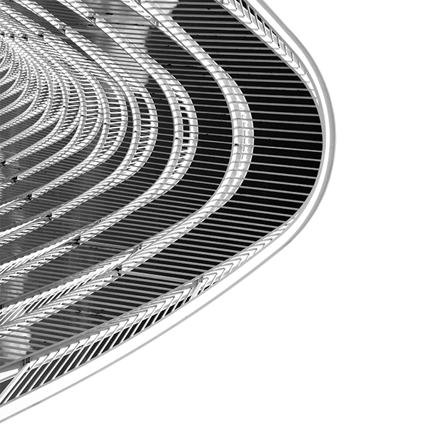
A spacecraft moving through plasma creates a plasma wake, which plays a significant role in differential charging between the front and back of the spacecraft. This wake needs to be modeled for debris-capture applications or docking routines. This wake can only be modeled accurately in 3D, an example is shown in Figure 1.
Plasma wake and plasma sheaths are consequences of plasma interactions with ambient fields and are only approximated in a BEM method, which has limited ability to calculate electric fields in relatively low-energy, dense plasmas found in low Earth orbit (LEO) or interplanetary orbits.

Figure 1. Plasma wake results shown in EMA3D® Charge.
Using Ansys Charge Plus and its PIC solver, together for surface charging produces predictively accurate simulations of the surface level in any orbit. To optimize your simulation further, integration with Ansys Systems Tool Kit (STK) enables the user to create a multidomain scenario to visualize the product or project in a realistic mission context.
Simulating Semiconductors Particle by Particle
Plasma enhanced chemical vapor deposition (PE-CVD) and plasma etching are experimental techniques that leverage multiphysics for product development in the semiconductor industry.
PE-CVD tackles the deposition of materials on the surface of a wafer, such as a thin coating. A chemical with free radicals is placed on the surface of the wafer and then the water is placed in a plasma chamber. A plasma may be generated from an ambient gas by driving a radio frequency (RF) source. The ions in the plasms interact with the surface of the wafer and the interaction with the radicals create byproducts. The influx of ambient gas and the outflux of byproducts is handled through valves that control the ambient flow of gas.
In order to simulate this process, various engineering disciplines are needed. These include:
- Fluid mechanics to model the gas motion in the chamber
- Electromagnetics to model the RF source and the field interactions with the plasma
- Plasma physics to generate and track the plasma dynamic near the wafer
- Chemistry for the interaction of the ions at the surface of the wafer
The PIC solver in Ansys Charge Plus coupled with its full wave FEM solver and additional Ansys multiphysics simulation tools bridge the gaps throughout the process and effectively connect plasma phenomena with EM physics.
Another challenge emerges because deposition rates rely heavily on the rate of collision between the ions in the plasma and the surface of the water. To tackle this simulation, the PIC models relativistic collisions within a species and between multiple species. The plasma distributions created by the PIC generate EM fields that are captured by the FEM, which is necessary to tackle the production of plasma sheaths that critically contribute to the deposition rates.
To complete the PE-CVD workflow, simply integrate the PIC and FEM solver technology into Ansys Fluent and Ansys Chemkin-Pro to begin computational fluid dynamics (CFD) and chemistry simulation. The co-simulation between the two solvers will leverage Ansys Systems Coupling 2.0 to generate a comprehensive simulation.
United All Parties and Particles
By engaging PIC solver technology, you experience deep integration at the physics level (coupling with Ansys Charge Plus with Fluent or Chemkin-Pro) and the user interface and workflow level (integrating the software into STK).
Ansys Charge Plus can also be integrated with Ansys Rocky particle dynamics simulation or Ansys EMC Plus (formerly EMA3D® Cable) to explore further physics-based simulation. To better visualize your project in realistic settings as you can in STK, you can use Ansys Charge Plus in conjunction with Ansys Discovery 3D simulation software, seen in Figure 2, or the Ansys ModelCenter model-based systems engineering (MBSE) platform.

Figure 2. Ansys Discovery simulation coupled with Ansys Charge Plus to simulate particles.
With Ansys Charge Plus you experience a more comprehensive physics simulation solution with solvers vetted individually, developed, and optimized using numerical methods, and paired through System Coupling 2.0. As a result, streamlined workflows accelerate simulation run time from setup to completion.
To read the full white paper on Ansys Charge Plus and its’ PIC solver, click here.
Learn more about what Ansys Charge Plus is capable of by clicking here.