Avoiding Signal Integrity Issues in High-Frequency PCB Design
A good brand reputation can lead to increased sales, customer loyalty, and investor confidence. However, if products fail to meet customer standards, they could potentially destroy reputations.
 The top five consumer electronics companies with a positive opinion from shoppers in 2024 Q1 are Bose, Philips, Samsung Galaxy, GE, and Dolby.
Designing printed circuit boards (PCBs) is of utmost importance, as they outfit nearly all consumer electronics. A PCB connects components and if it malfunctions it could lead to reduced bandwidth and entire device failures. Additionally, a faulty PCB can also potentially pose a safety risk by overheating or causing electrical hazards. To maintain a functioning PCB, you need to keep signal integrity or arrange and connect the board in a way that minimizes signal interference.
Maintaining Signal Integrity
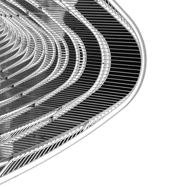
As technology advances, high-frequency PCBs are becoming more common. These high-speed boards operate at 1 GHz or higher and in the microwave and radio frequency (RF) ranges. They work well in complicated electronics because they are compact, reliable, cost-effective, and they maintain signal integrity. It is the last part, signal integrity, that is the key to successfully designing PCBs.
Signal integrity is a measure of the quality of an electrical signal as it travels along a transmission path. Traveling signals encounter factors that will affect how it moves. Several methods can weaken or loop back a signal on itself. A board that does not avoid these issues could degrade and die eventually.
Poor Signal Integrity
There are several causes of poor signal integrity in a PCB such as propagation delays, attenuation, voltage fluctuations, and signal characteristics. To achieve a desired signal integrity level, designers should keep four main factors in mind. They are electromagnetic interference (EMI), crosstalk, ground bounce, and impedance mismatch.
- Unwanted electrical signals, frequencies, or electromagnetic radiation that can impact a device. This is called EMI. The signals came come from the device itself or external issues such as from another device or ambient radio waves. PCB designers need to reduce EMI from individual components to ensure signal integrity is not compromised.
- Crosstalk develops when a signal transmitted on one circuit or channel creates an undesired effect on another circuit or channel. Typically, this happens on PCBs when electromagnetic coupling between traces causes interference and noise. Traces that are too close together usually cause this problem. Crosstalk is inevitable, but it can reduce it to a level where it does not affect signal integrity significantly.
- Ground bounce is a type of noise that occurs when there is a difference in ground potentials at various points on a circuit. This is a problem especially in high-speed or high-frequency devices, causing switching and double-switching reducing the signal integrity.
- Impedance matching is the ability of a circuit to effectively transfer signals from the source into the routing and then from the routing to the load. Reflections can exist along the route between the source and the load if you do not do this correctly, creating an impedance mismatch. This lowers signal integrity because the signals interfere with the transmitted signal as they propagate back and forth in the trace, causing data jitter and a reduction in the signal-to-noise ratio.
Solving Signal Integrity Problems
Resolving any potential signal integrity problems early in the design process is key to having a successful product launch and fixing problems starts with simulation. Ansys EMC Plus is the premier software tool for EMC/EMI analysis. Unlike other tools that only look at individual components, EMC Plus can analyze full platforms and handle complex geometries and interactions like PCBs.
EMC Plus evaluates signal integrity and how digital signals are affected by cable definitions and external electromagnetic noise. Other capabilities include:
- Shielding effectiveness analysis
- EMI crosstalk between cables
- Current return network optimization
How Ansys EMC Plus Works
EMC Plus uses a hybrid approach that combines three solvers to evaluate the full platform model, including 3D fields, cables, and nonlinear circuits. The finite difference time domain (FDTD) method captures the complex interactions between the 3D fields and the platform, accounting for the effects of shielding, apertures, and slots. A modified multiconductor transmission line (MTL) solver models the effects of cable routing, twisting, and bending, as well as accounts for coupling between cables and 3D fields. A transient nonlinear circuit (TNC) solver accounts for the effects of voltage and current sources, loads, and switches.
A forgiving mesh allows EMC Plus users to solve extreme geometric complexity without extensive user effort to clean and prepare the geometry for simulation. The software also includes automated workflows and wizards and GPU acceleration for faster results. This includes automatic PCB import from Ansys Electronics Database as seen in Figure 1.
EMC Plus automatically assigns the linear components including resistors, capacitors, and inductors, and the electromagnetic material properties. Figure 2 shows the resulting fields from inside the enclosure.

Fig 2. Resulting fields inside the enclosure using automatic PCB input in Ansys EMC Plus.
EMC Plus also imports and merges 3D CAD geometry and cable database information automatically for easy EMI/EMC analysis and provides seamless integrations with other Ansys tools.
Get Started
Headlines about failing PCB boards and products could not only cost companies money, but their reputation.
At EMA, our consultants are ready to assist brands in EMI/EMC certification, design, and qualification of systems. EMA staff have served as EMC lead or supported many high-profile programs in the past. Clients include the Department of Defense and NASA Prime contractors.
EMA will support you by:
- Writing EMI/EMC control plans
- Writing testing plans, executing testing, and writing test reports
- Determining the attenuation of energy between source and victim
Click here to learn more about how we can help.
EMA developed EMC Plus and releases new features every six months. Ansys is the exclusive seller. To learn more about what is possible with EMA and EMC Plus, click here.