Determining ESD Risk in Cell Phones with Ansys Charge Plus
The shock from static electricity to the human body can be jarring, but it is nothing more than a nuisance. However, that same shock can cause bigger problems for many electronic devices.
That shock is also known as an electrostatic discharge (ESD) event. ESD has been a problem in industry for centuries. In the 1400s, European and Caribbean military forts used static control procedures and grounding devices to prevent the unintended ignition of gunpowder stores. At the end of the industrial revolution, U.S. paper mills had implemented basic grounding, flame ionization techniques, and steam drums to help keep static electricity away from the paper web as it went through the drying process.
Nearly every industry has had to deal with ESD, including petrochemical, pharmaceutical, agriculture, plastics, and electronics. With the advancement of electronics technology, new ESD problems are developing. As devices get smaller, they have an increased sensitivity to ESD. A smaller device means a small chip, reducing the silicon geometry via wafer processing.
If you find your cell phone keypad or buttons suddenly don’t work, damage from an unprotected ESD event could be to blame. The same phenomena can also cause a connected USB device or Ethernet cord to suddenly stop working.
Testing for ESD during the cell phone design process can help designers pass EMC compliance evaluations. Ansys Charge Plus is capable of finding arcing between an ESD gun and the printed circuit board (PCB) in a cell phone. This article describes the general workflow of how to simulate ESD events using Charge Plus.
Setting up the Simulation
To begin the simulation, the user needs to open the cell phone model in Charge Plus. To find the arcing between the ESD gun and PCB, a gap needs to be created between the two parts. In this example model, this is done by deleting the power button.
Once the cell phone model is ready it can be imported into the ESD gun model. The importing process is seen in Figure 1. The cell phone geometry will need to be shifted so that the area of interest is under the ESD gun tip. Organizing the separate models into individual folders in Ansys Charge Plus is extremely useful if at any point they are being worked on independently.
Figure 1. Importing the target model into the ESD gun model.
The next step is to find the domain. This is done by clicking on the domain button and setting the parameters. Then the breakdown region will be defined, marking the area where arching will occur (Figure 2).
Figure 2. Steps needed to be taken to define the arcing region.
With the model set up, material properties can be assigned to the target model. In addition to defining new material, existing material will be assigned to the cell phone model. Figure 3 shows how this is done. Choosing contrasting colors can aid in the visual comprehension of complex models.
Figure 3. Defining and assigning materials to the geometry.
Setting Up Probes
A current probe will be placed between the gap in the model and the tip of the ESD gun. Next, two animation planes need to be defined. Using two planes helps provide a more detailed look at the arcing. This process is shown in Figure 4. When ready, animation probes for the electric current on the PCB will be placed in the model. Some components will need to be hidden to correctly select the PCB.
Figure 4. Process to add animation planes.
The last probe that needs to be added is the voltage probe (Figure 5). To aid in accurately selecting the PCB, defining a geometric point is helpful to provide the voltage probe a position to snap to.
Figure 5. Process to add a voltage probe.
When setting up probes, there are some things to keep in mind:
- Bulk Current: Generally, the normal direction should be orientated so that the probe is a plane instead of a series of lines.
- Animation Probes: Setting up two vertical animation planes allows for a more detailed animation of arcing. In addition to having the option to set the probe type to air conductivity, which is essential for the visualization of air chemistry breakdown, it can also be set to electric current which is extremely useful for examining the effects of discharge on a PCB.
- Voltage Probe: Creating the second geometric point is useful for making sure the positive assignment of the voltage probe snaps to the intended location.
Running the Simulation
The simulation can be started as soon as all the probes are set. The value of a standard voltage for an ESD test varies and is product and industry dependent. The ESD model can be calibrated to fit these different demands.
Data Visualization
When the simulation is complete, the results will be plotted in charts like the ones in Figure 6. The chart on the left is the voltage probe and the one on the right is the current.

Figure 6. Data visualization of voltage (left) and current (right).
Review the Voltage Probe graph and Bulk Current graph and compare the first iteration (AI case with an amplitude = 1.2E+08) to the results shown in Figure 7. If they agree change the phone case to the Dielectric material and compare the results. The voltage of the first dielectric case iteration should follow the AI curve until the voltage drops, which indicates that arcing is not occurring. The distance increases as arching I s happening between the tip of the ESD gun and the PCB, instead of between the tip and the aluminum case. To induce arcing, increase the amplitude of the waveform to 2.4E+08 from 1.2E+08 and compare the results.
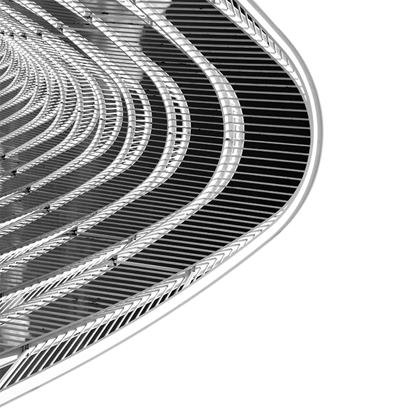
Figure 7. is a visual representation of when a breakdown will happen at different amplitudes. In this case, the red color shows a breakdown.
Conclusion
ESD is a real threat for electronics, so it is important to make sure levels stay below a certain threshold. The ESD gun simulation in Ansys Charge Plus makes it possible to determine when a breakdown will happen. Materials can easily be changed, and voltages can be set for any project. The ESD gun model works with more than just cell phones, but also other electronics with a PCB.
Ansys Charge Plus is a part of the Electronics Plus Family built by EMA. It is sold exclusively through Ansys. To learn more, click here.