New Physics-Based Space Environment Simulation and SEY Measurement for Accurate Charging Risk Assessment
Topic:
New Physics-Based Space Environment Simulation and SEY Measurement for Accurate Charging Risk Assessment
Presenters:
Kevin-Druis Merenda, EMA Principal Scientist I
Justin Christensen, EMA Staff Scientist
Abstract:
Electro Magnetic Applications, Inc. (EMA) continues to distinguish itself through ongoing advancements in Ansys Charge Plus and the Space Environment and Radiation Effects (SERE) Lab, delivering a uniquely integrated set of capabilities that are not available through any other provider.
The SERE Lab provides a controlled test environment that recreates realistic space conditions enabling direct measurement of spacecraft charging, electrostatic discharge (ESD), radiation effects, and material behavior under mission-relevant scenarios. At the same time, Charge Plus delivers a physics-based, 3D simulation capability for modeling surface and internal charging, particle transport, and arcing across complex systems. By tightly coupling these capabilities, EMA creates a closed-loop workflow where measured data from the SERE Lab informs and validates simulation models, and simulations guide targeted testing. This combined approach moves beyond standalone software or isolated testing, providing customers with higher-fidelity predictions, reduced risk, and engineering confidence grounded in both physics and proof.
In this session, we introduce new advancements in space environment simulation and secondary electron yield measurement.
Advancement #1: Space Environment Simulations in Ansys Charge Plus
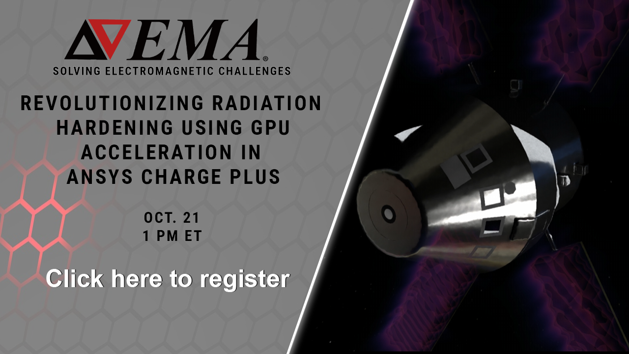
Through partnerships with NVIDIA and Synopsys, EMA has GPU‑accelerated Charge Plus and integrated it with electronic design automation (EDA) tools, enabling mission‑to‑silicon workflows for radiation hardening and EMC in space and defense.
This integration with Synopsys tools like TCAD Sentaurus Design, allows end‑to‑end modeling from spacecraft and electronics down to silicon, capturing total ionizing dose (TID), linear energy transfer (LET), and device‑level response to high‑energy Galactic Cosmic Rays (GCRs), while accelerating design iteration and decision‑making.
In part one, see how to model radiation effects from orbit to silicon in a single workflow. We will demonstrate the mission‑to‑silicon workflow through an end‑to‑end analysis of GEO electrons interacting with the satellite, electronics, and PCB, culminating in silicon‑level ionizing dose and device response.
Advancement #2: New Secondary Electron Yield Measurement Capability
Secondary electron yield (SEY) is a key material property in spacecraft charging, determining how energetic electron impacts influence whether a surface charges positively or negatively. Inaccurate SEY data directly compromises charging predictions, increasing risk in harsh radiation environments, especially for new materials lacking well‑characterized properties.
EMA’s SERE Lab has established dedicated SEY measurement for spacecraft charging, making EMA one of the few organizations with both insulator SEY testing and integrated simulation capabilities. Using a pulsed, low‑current electron beam and custom instrumentation, EMA characterizes insulating flight materials across relevant energy ranges (50–5000 eV) while preserving surface state for accurate results. This measured data feeds directly into simulation workflows, enabling more reliable, material‑specific charging risk assessments.
You will walk away with:
- A clear understanding of mission-to-silicon workflows for modeling radiation effects using Ansys Charge Plus
- Insight into how GPU acceleration and EDA integration are improving simulation speed and design iteration
- Knowledge of secondary electron yield (SEY) measurement techniques and their impact on charging accuracy
- A practical view of closed-loop validation, combining simulation with SERE Lab measurement data