Beginner’s Guide to EMI/EMC Simulation

As electronic devices become more complex and the market more competitive, the consequences of overlooking electromagnetic compatibility (EMC) and electromagnetic interference (EMI) reach far beyond the engineering team, they directly affect the customer. Devices plagued by EMI/EMC issues can suffer from unreliable performance, unexpected malfunctions, or even total failure during critical moments. This not only diminishes user confidence but can also jeopardize customer safety and satisfaction.
With around half of all devices failing the first round of compliance testing, using simulation to determine EMI/EMC is no longer optional, it is essential to avoid pitfalls, getting you to market on time and on budget.
This is a guide on how to begin using simulation. It includes:
- Simulation goals
- Applications areas
- Reliable software
- Ease of use
Step 1: What is the Goal?
Engineers new to simulation often seek to solve specific issues. For example, why current or past platforms fail to achieve certification or predicting how their unit will perform in certain environments. The first step to starting a simulation campaign is to define the goal of simulation simply by asking ‘what do I want to analyze?’
Simulation software enables you to explore the following areas:
- EMI/EMC
- Radiated emissions/ immunity
- Conducted emissions/ immunity
- Shielding effectiveness
- Cable to RF system coupling
- Electromagnetic environmental effects (E3)
After a goal has been defined, it’s time to decide when simulation will take place. It is important to note that replicating a test environment requires time and effort, making it an ambitious goal. Teams achieve greater success when they use simulation proactively throughout the design process, rather than reactively in response to problems. Establishing this practice early allows for smoother implementation.
Designers can use simulation to reinforce strong design practices. Values should be extracted from simulations throughout the setup process, not just at the end when a final model has been finalized.
Step 2: Preparing for Simulation

EMI/EMC simulation of electronic devices should include printed circuit boards (PCBs), cables, and mechanical enclosures. As the second step in starting simulation, identify components and where they are placed in your product. Creating preliminary designs, PCB layouts, and schematic diagrams will help you:
Identify likely problem areas, allowing you to focus simulations where they matter most
Accurately represent electrical characteristics leading to more accurate results
Simulation use extends well beyond the realm of consumer electronics. Other application areas include:
- Aerospace and defense
- Automotive
- Energy
- Heavy industry
- Spacecraft
Step 3: Choosing Software
The next step is to choose a simulation tool. A variety of software is available for simulating EMI/EMC, but Ansys EMC Plus delivers the greatest benefits in the shortest time. Unlike other programs, EMC Plus simulates EMI/EMC across entire platforms, not just isolated components. The software models complete systems including PCBs, cables, enclosures, and antennas. Figure 1 is a look at the EMC Plus interface, which is built in Ansys Discovery.

Fig. 1. An electronic device imported into Ansys EMC Plus
EMC Plus combines hybrid finite-difference time-domain (FDTD), multi-conductor transmission line, and Nexxim transient circuit solving methods. The FDTD approach solves Maxwell’s equations directly in the time domain, making it ideal for tackling broadband, complex, and large-scale electromagnetic problems. FDTD also allows users to handle non-linear materials and arbitrary geometries with ease, and its efficient scaling supports large platforms.
Easily integrate EMC Plus with other Ansys software including:
- Granta
- HFSS
- optiSlang
- SIwave
Step 4: Easy Advanced Modeling
Starting simulation is fast with EMC Plus. The software’s full CAD integration sets it apart from competitors by enabling users to build precise models efficiently. Users can import files directly from Zuken E3, VeSys, Capital Harness, and other mechanical CAD without needing any cleanup. Import also includes all 3D cable routing data such as electrical definitions. Figure 2 shows the import process.
Next, engineers can also model cables within EMC Plus using a comprehensive and highly automated workflow, which simplifies simulation, even for first-time users. The software enables users to represent cable geometries in detail, including:
- Shields
- Overbraids
- Branches
- Terminations
The video in Figure 3 shows how easy it is to assign different material definitions in a radiated emissions simulation.
Speedy Results
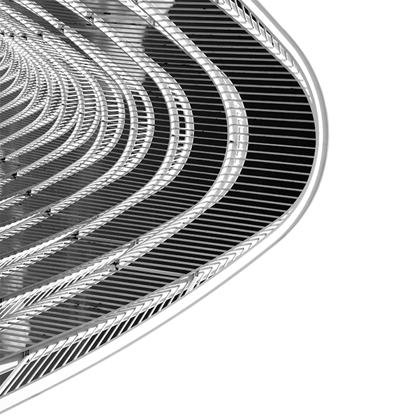
EMC Plus speeds up simulation through a combination of a variable grid mesh and GPU acceleration. The Cartesian-style mesh adapts dynamically to the model’s geometry, assigning smaller mesh cells to regions with intricate details, such as cable junctions, PCB traces, or connector interfaces, and larger cells to areas with less detail. This can be seen in Figure 4. This selective refinement reduces the total number of mesh cells which in turn accelerates simulation speed. The fault-tolerant mesh eliminates the need for users to manually clean or simplify the geometry before running simulations.

Fig. 4. Variable grid mesh in Ansys EMC Plus.
Users can benefit from the GPU-accelerated solver on both Linux and Windows platforms, including standard desktop systems. Benchmarks show that inexpensive GPUs simulate four times faster than multi-core CPUs alone.
Analyzing Results
Automatically generate animations and 2D field plots in both time and frequency domains, enabling intuitive analysis of electromagnetic behavior. These visualizations identify hotspots, coupling paths, and shielding effectiveness without requiring manual post-processing. EMC Plus also includes interactive field viewers to display electric and magnetic field distributions, making it easier to validate simulation accuracy and communicate findings. Figure 5 shows an example of how to view radiated emissions results.
Validation
EMC Plus has undergone rigorous validation, including physical testing of an electronic device for radiated susceptibility. The simulation results were compared to lab measurements with excellent correlation. Read more about this validation campaign by clicking here.
USE CASE: Make sure to read the article “Ansys and EMA Help Intel Achieve the Impossible: EMI Simulation of an Entire Server” for a closer look at how EMC Plus can be used in electronics simulation.
Final Analysis
EMI/EMC testing is a critical step in the development of electronic systems. Unintended emissions can disrupt functionality, compromise safety, and violate regulatory standards. Early EMI/EMC simulation helps identify and mitigate these risks reducing costly redesigns and delays.
Full platform simulation is an iterative journey that reveals valuable engineering insights throughout the process. Rather than substituting sound design principles, simulation reinforces them. With Ansys EMC Plus, this approach is not only achievable but streamlined, empowering engineers to build smarter, faster, and with greater confidence.
Electro Magnetic Applications, Inc. (EMA) releases updates to EMC Plus twice a year. In addition to maintaining the software, EMA provides comprehensive support for EMC Plus users ensuring successful deployment and high-impact simulation outcomes. Support includes mentoring, consulting, and training services for help navigating everything from CAD import and cable modeling to certification workflows.
Contact EMA today and begin your journey!