Rethinking Optics- How EMA is Supporting the Push for Metalenses
Most of us use a smartphone daily. It lets us connect with loved ones, send emails on the go, and take pictures wherever we are.
Today’s smartphone cameras are producing quality images, closing the gap between phones and traditional cameras. Built-in cameras, more specifically the lens system, are one of the most expensive parts of a cell phone. Experts expect the average cost of a cell phone to rise to more than $1,400 by 2027. But, could relief be on the way? Electro Magnetic Applications (EMA) along with the University of Massachusetts Amherst believe metalenses are the future of smartphone technology.
Supporting Innovation
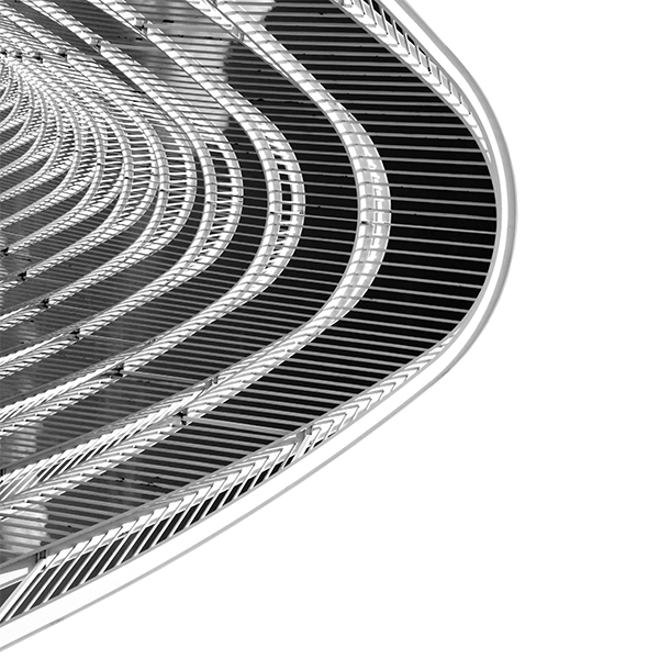
Metalens is short for metasurface lens. They are commonly made out of a flat sheet of silicon dioxide or similar material topped with posts, or nanostructures, as Figure 1 shows. Traditional lenses rely on the curvature of their surface to refract or focus light. Metalens do not take this approach and instead use carefully engineered patterns of nanostructures to control the phase and amplitude of light across the surface of the lens. This method allows for precise control over the direction and properties of light, giving metalenses the ability to perform a wide range of optical functions. Metalens are slimmer than a traditional lens, measuring about 1/100th the thickness of a human hair.

Fig. 1. Highly efficient metalens. Courtesy: UMass Amherst.
“When you think about optics, we’ve been doing it the same way for hundreds of years,” Jim Watkins, UMass Amherst professor of polymer science, said. “It’s amazing that the same principles that Galileo used to build the telescope are still the ones that we use to focus light.”
Innovation leaders are supporting EMA and UMass Amherst’s quest to learn more about this new technology. The Massachusetts Collaborative (MassTech) announced in late 2023 that it would be awarding a $5 million grant to the two partners to boost advanced optics technology design and production.
The Role of UMass Amherst
The grant establishes the first publicly accessible metalens manufacturing and design/testing facility at UMass Amherst. The lab will support testing, research, and production of optical technologies. Nanoimprint lithography equipment manufactures metalenses at a significantly lower cost compared to the semiconductor process. This optical technology has applications in biotechnology, defense, aerospace, environmental monitoring, and general electronics.

Fig. 2. MassTech, UMass Amherst, and EMA come together to celebrate a $5 million grant for advancing optical technologies. Courtesy: Thom Kendall.
“Optical technologies are essential in the 21st Century, acting as the backbone for transformational industries ranging from semiconductors to mobile technologies, medicine to national defense,” Pat Larkin, director of the Innovation Institute at MassTech, said during the award presentation. “That’s why it is critically important to expand collaboration and partnerships in this space, to encourage increased engagement between research institutions, and private industry.”
The Role of EMA
For its part, EMA will test metalenses for durability and viability to let researchers know the limits of a particular design.
“You have all the ideas and thoughts and you come to UMass Amherst, and you manufacture it,” Justin McKennon, EMA Principal Scientist II, said. “Our way of answering the question is how is it going to work where you’re trying to use it.”

Fig. 3. EMA Principal Scientist II Justin McKennon addressing the crowd during the grant announcement ceremony. Courtesy: Thom Kendall.
Designing Metalens
As an option to improve complex imaging and illumination device performance while reducing system size and weight, more people are seeing metalens. Instead of several tradiational optical components, one metalens can suffice.
“If you pull out your iPhone and you look at these big bumps on the back,” Watkins says. “They’re not a single lens, there are five lenses in that train because each of those lenses has to be combined. If we can miniaturize optics, think about what you can do with that. One, you can make the bumps go away on your iPhone.”

Fig. 4. Professor Jim Watkins showing an iPhone camera lens system during the panel “BIC Presents: From Lab to Market.” Courtesy: Berkshire Innovation Center.
The nanoimprint lithography equipment process is similar to using a stamp. The semiconductor wafer forms a pattern, and it stamps out copies in a polymer. Watkins says this one wafer can make 100,000, 200,000, or even 1 million devices at the same time. This method is not only cost-effective but easily replicates nanoscale patterns with high precision. This technology is not currently available in any public facility in the U.S.
How the nanostructures are arranged determines the way a metalens will behave.
“If you want to change the wavelength, you change the spacing,” Watkins said. “There you get all the degrees of freedom in optics without playing with multiple lenses just by rearranging the size and shape of these posts.”
Testing For REal World Use
EMA will test the limits of the metalenses at its Pittsfield, Massachusetts location using simulation and physical experiments.
The testing process starts with simulation. EMA developed and maintains the simulation tools Ansys EMC Plus and Ansys Charge Plus to learn more about how products behave in the space plasma environment, semiconductor processing plasmas, and electromagnetic environmental effects. Designers can plug sketches right into the simulation tool and see how they will react in various electromagnetic environments. This includes analyzing the impacts of lightning and radar.
“Without the ability to do simulations and iterate on things quickly, you’re going to get stuck in a lab forever,” McKennon said. “We can learn what the limits of a particular design are. Then we can put it in space, we can put it underwater, we can put it on a boat or a train or in a car and understand if we are ever going to hit that limit and if we do hit that limit what ways can I tweak my design without having to go back to fab [fabricate] something new.”
Physical Testing
EMA will also conduct physical testing of the metalenses in a special testing chamber to evaluate:
- How metalenses age and degrade
- How design features change their electrical properties
- How metalenses break and fail
Funds from the grant will build on EMA’s current measurement and characterization equipment, the Space Environment and Radiation Effects (SERE) commercial test chamber, shown in Figure 5.

Fig. 5. EMA’s current testing and characterization facility named SERE for space environment and radiation effects.
McKennon expects it will be about three years before the lab is ready for its first commercial customer. He says that, like how EMA first used SERE, there is no blueprint for getting started.
“We just roll the sleeves up and engineer it,” McKennon said. “There are no standards because this is new, there are no requirements, there are no certifications.”
Starting in 2024, McKennon believes the lab will have proton capabilities, which is something he says no commercial research facility in the U.S. has the ability to do.
Preparing for the Future
A third piece of the grant program is getting students the chance for hands-on experience.
Higher education partners include Northeastern University, Springfield Technical Community College, and Berkshire Community College.
Since this is an emerging technology, McKennon says students will get training that individuals currently in the workforce do not have while having the opportunity to help build the program.
“This is an area where we have an opportunity to start and do this correctly,” he said. “If we’re the only location in Massachusetts that has the ability to adapt a curriculum to what the industry needs, then they’re going to come here, I think that’s what we want.”
The Berkshire Innovation Center (BIC), where EMA’s lab is located, will also provide workforce development opportunities for students and young professionals.
“I think the other thing that an initiative like this can do is it can teach the kids that manufacturing can be exciting, it can be interesting,” Watkins said. “You can show them what it’s [the equipment] going to do, you can make the lens, and then it works, and it looks interesting.”
REthinking Optics
Rethinking optics opens up an entirely new opportunity. It can not only redesign cell phone cameras but also make other devices more efficient such as:
- Lidar for 3D sensing in autonomous vehicles and facial recognition systems
- Augmented and virtual reality headsets
- Medical devices like endoscopes and microscopes
- Surveillance systems such as IR and machine vision cameras
“I think I’m most excited about learning what knobs that you can turn on a design and what those knobs actually do because I don’t think anybody really knows that,” McKennon said. “If I changed this little piece of an ingredient, did I add 10 years to my space survivability? I don’t know. That’s going to be something that none of us know the answers to. It’s going to be really kind of a fun part for all of us to learn as we go forward.”
Make sure to check ema3d.com for new details as we continue to work on this project.
The BIC hosted a panel “BIC Presents: From Lab to Market” where McKennon, Watkins, and Larkin all took part talking about developing metalens technology and the impact on industry. You can watch the panel for yourself below or by clicking here.